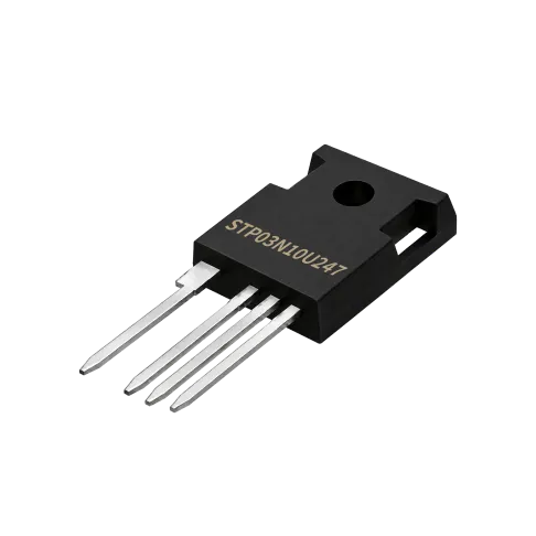
STP03N10U247 100V 3mΩ SGT MOSFET
Specifications
Product details
Overview
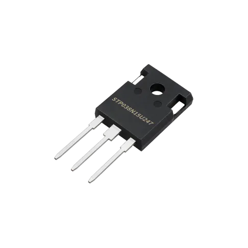
The STP03N10U247 is a 100V N-channel enhancement-mode SGT MOSFET manufactured with advanced double trench technology, combining low on-resistance, low gate charge and superior switching performance. It supports a maximum continuous drain current of 180A at 25℃ (package limited; 239A silicon limited) and 720A pulsed, with RDS(on) of 3mΩ max (2.7mΩ typ) at VGS=10V, a typical gate threshold voltage of 3V (2~4V), a typical total gate charge of 131nC and a reverse transfer capacitance of only 110pF. The device handles a single-pulse avalanche energy of 784mJ, dissipates up to 357W, and its body diode achieves a reverse recovery time of 80ns with 195nC reverse recovery charge. Operating over a -55~+150℃ junction temperature range and housed in a TO-247 package, it is an ideal choice for BMS and high current switching applications.
Features
- N-channel enhancement-mode SGT MOSFET with advanced double trench technology
- Fast switching with low on-resistance: RDS(on) 3mΩ max (2.7mΩ typ) at VGS=10V
- Max continuous drain current 180A (TC=25℃, package limited), pulsed drain current 720A
- Low gate charge: total gate charge Qg 131nC typ
- Low reverse transfer capacitance: Crss 110pF typ
- High avalanche ruggedness: single-pulse avalanche energy EAS 784mJ, max power dissipation 357W
- Body diode reverse recovery time 80ns, reverse recovery charge 195nC
- Operating junction temperature -55~+150℃, TO-247 package
- RoHS product
Typical Applications
- BMS (Battery Management Systems)
- High current switching applications