EV DC Fast Charging IC & Semiconductor Solutions
Overview
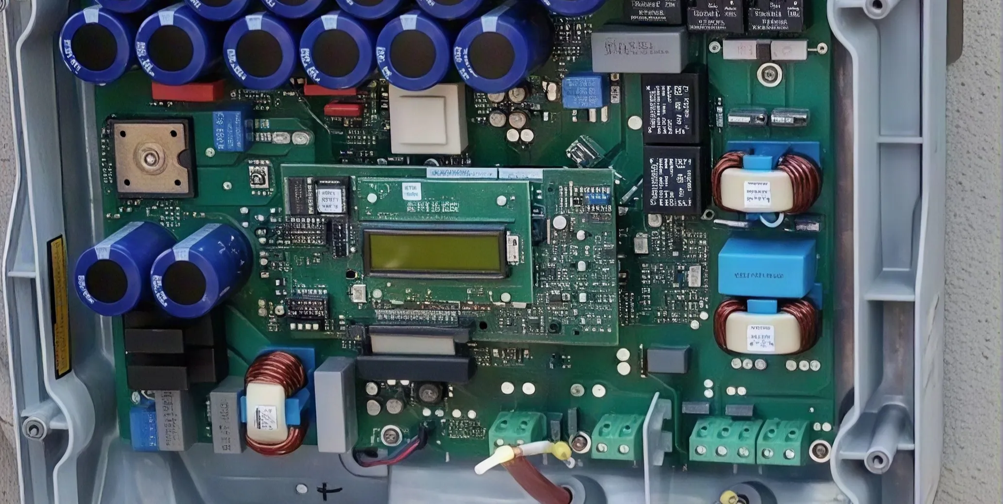
The rapid expansion of the new energy vehicle market is driving DC fast charging modules toward higher power density and higher efficiency. 40 kW and 60 kW modules have become the mainstream configuration for highway service areas, urban public charging stations, and commercial fleet depots, imposing stringent requirements on conversion efficiency, power factor, harmonic distortion, and grid compatibility.
In a typical 40/60 kW DC fast charging module, the front-end three-phase power factor correction (PFC) stage and the isolated DC-DC stage place demanding requirements on the switching devices: the PFC stage must maintain high efficiency and low harmonic distortion at high input voltage, while the DC-DC stage must regulate a wide output range from 200 V to 1000 V to accommodate different battery architectures.
System Architecture
Mainstream 40/60 kW charging modules adopt a two-stage architecture. The front end is a three-phase Vienna PFC topology in which each phase leg combines a high-speed active switch with a diode bridge; the rear stage is a full-bridge LLC resonant converter whose primary-side bridge is typically built with 1200 V-class devices.
In the Vienna PFC stage, the STG80T65FDK7 serves as the active switch of each phase and operates at the semi-bus voltage divider position, where it sustains only half of the total DC-bus voltage. This positioning relaxes voltage stress, allowing a 650 V device to operate safely in systems with an elevated DC link, while its low conduction and switching losses directly shape the module efficiency.
Recommended STST ICs
STG80T65FDK7 — 650 V / 80 A Trench-FS Gen7 IGBT with fast-recovery diode, TO-247. Engineered for the Vienna PFC stage of high-power charging modules, it combines an ultra-low saturation voltage, optimized switching behavior, and robust thermal capability up to a 175 ℃ junction temperature.
| Parameter | Typ. | Unit |
|---|---|---|
| Collector-Emitter Voltage VCES | 650 | V |
| Rated Current IC (Tc = 100 ℃) | 80 | A |
| Saturation Voltage VCE(sat) (Ic = 80 A, 25 ℃) | 1.60 | V |
| Gate Charge QG (Ic = 80 A) | 146 | nC |
| Total Switching Loss Ets (25 ℃) | 2.20 | mJ |
| Diode Recovery Charge Qrr (IF = 80 A) | 1.7 | μC |
| Thermal Resistance RθJc (IGBT) | 0.32 | ℃/W |
| Operating Junction Temp. Tvj | –40 to +175 | ℃ |
| Package / Ordering Code | TO-247 / STG80T65FDK7U247 | — |
Key Advantages
- Low conduction loss: VCE(sat) of 1.60 V at 80 A, rising only to 2.05 V at 175 ℃, delivers excellent heavy-load efficiency.
- Low switching loss: total Ets of 2.20 mJ (Eon = 1.45 mJ, Eoff = 0.75 mJ) suits 20–50 kHz high-frequency PFC operation.
- Easy gate drive: QG of 146 nC with fast switching (tr = 43 ns, tf = 54 ns at 25 ℃) reduces driver design effort.
- Reliable paralleling: positive temperature coefficient and 175 ℃ junction capability support natural current sharing in compact charging cabinets.
- Integrated fast-recovery diode: Qrr of 1.7 μC simplifies the gate drive and reduces external snubber components.
FAQ
Why can a 650 V device be used in a high-voltage charging module?
In the Vienna PFC topology, the STG80T65FDK7 sits at the semi-bus voltage divider point and sustains only half of the total DC-bus voltage, keeping the stress within its 650 V rating even when the full bus voltage is high.
Is the STG80T65FDK7 suitable for the DC-DC (full-bridge LLC) stage?
Not recommended. In a full-bridge LLC primary side, each switch must sustain the full DC-bus voltage (typically 700–800 V), which leaves insufficient margin for a 650 V device. A 1200 V-class IGBT is recommended there; the STG80T65FDK7 is positioned for the Vienna PFC stage.
Does STST provide reference designs and evaluation support for Vienna PFC?
Yes. STST provides reference design documentation, device selection guidance, and dedicated FAE support for the Vienna PFC stage to shorten the charging-module development cycle. Contact the FAE team for details.
How much do losses increase at high temperature?
Per the datasheet, as junction temperature rises from 25 ℃ to 175 ℃, total switching loss Ets increases from 2.20 mJ to 2.72 mJ (about 24%). Thanks to the low RθJc of 0.32 ℃/W, the actual temperature rise remains controllable.